

|
||||||||||||
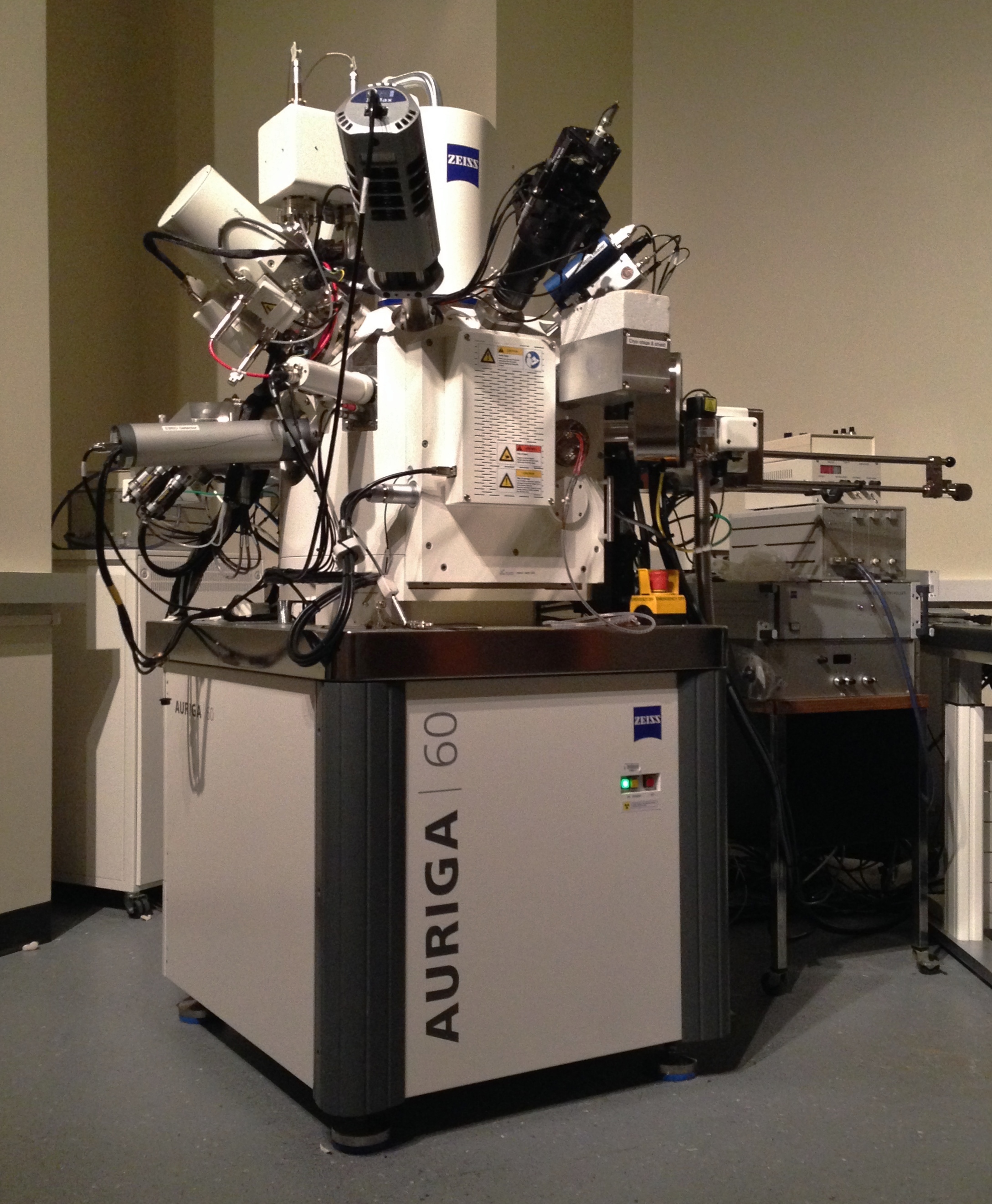
| Zeiss Auriga 60 High Resolution Focused Ion Beam & Scanning Electron Microscope |
| Applications: | High resolution FIBing, imaging, compositional and structural analyses Auto slice & view 3-D reconstruction of images, XEDS maps and EBSD phases/orientations Nano-fabrication TEM sample prepataion Cryo SEM Correlative microsocpy Bright field & dark field scanning transmission electron microscopy (STEM) EBIC |
| Accelerating Voltage and Beam: | e–: 0.1-30kV; 4pA-100nA i+: 0.5-30kV; 1pA-50nA |
| e– Beam Column: | Schottky FEG Gemini column |
| i+ Beam Column: | Liquid Ga Orsay Physics Cobra FIB column with 2.5 nm resolution |
| XEDS/EBSD: | Oxford Synergy X-MAX80 & EBSD |
| Cryo SEM: | Leica EM VCT100 Vacuum Cryo-Transfer System |
| Location: | ISE Laboratory – Room 174 |